For my next video, I thought I’d investigate the topic of SDR – software-defined radio. My career started in wireless, mainly thanks to my hobby of amateur radio. I initially trained as a Merchant Navy radio officer and worked for BP on big supertankers. I’ve had plenty of experience with traditional RF engineering techniques but have wanted to explore and get ‘hands-on’ with SDR and related topics for a while.
This is the first in a series of videos about SDR. After a short introduction to SDR, I unbox the ADALM-PLUTO from Analog Devices.
Subsequent videos will explore popular modulation techniques and practical receiver & transmitter designs. Along the way, we’ll also cover aspects of antenna design, measuring return loss, and investigate communication through the amateur radio QO-100 satellite.
Vast armies of sensors are crucial to feeding IIoT monitoring and analysis applications. Powering these edge nodes is increasingly a channel. Even though modern microcontrollers exhibit ultra-low power consumption characteristics, a battery would need to be replaced at some stage, the total cost of which is typically more than the sensor. Provisioning line/mains power infrastructure is equally expensive.
How about energy harvesting? Could this provide a viable power source? What about harvesting ambient RF energy?
In this video, we investigate the potential for powering IIoT sensors using this approach.
The electronics industry is awash with highly integrated modules and system-on-chip (SoC) devices. Are these only a short-term event or will they shape the industry’s future?
A few months ago my son purchased his first motorbike. Like all new things, it is his pride and joy, and the thought of losing it led him to ask me if I could build a GPS tracker for it. Naturally, I said yes!
I started my electronics studies in the mid-1970s, and valves (tubes) were still very much on the curriculum. Digital logic was still in its infancy back then, but it gathered momentum extremely quickly. Roll the clock forward many years, and I’m in a position, like many other engineers or makers, to confidently rise to the challenge of building a GPS asset tracker. So how come?
In short, today anyone can buy a highly integrated set of modules and SoCs and build such a device. I’m not going to go into the design of the tracker here, although I might save it for another post. The design criteria were fairly simple. Build a tracker that would be powered off the motorbike’s electrics that could be interrogated by text message to respond with its current latitude and longitude location. After a bit of research, I selected two boards — the Arduino MKR GSM 1400 and an Arduino MKR GPS shield. The hardware is illustrated above. With the help of a pay-as-you-go SIM card for the GSM module, some library code and examples from the Arduino website, I had a prototype running, accurately reporting the location.
I think we should reflect on this achievement for a moment.
When powered up, the GSM module attached itself to the cellular network and sat waiting to receive a coded text message. Likewise, the GPS shield sat scanning the sky above for constellations of GNSS satellites. When a valid code was received by the GSM module it took the current location and replied to the sender with the bike’s location in a text message. Data is presented in a Google Maps format that shows the location on a map.
I consider myself a fairly capable engineer and coder, but the sheer complexity of tasks involved in establishing communication on a cellular network is beyond me. I could probably hack my way around the GPS receiver, but not in a couple of hours.
Commoditization is driving the electronics industry forward
The fact I could build a device of this nature is thanks to electronics manufacturers and silicon vendors developing highly integrated and functionally rich semiconductors and modules. The mass commoditization of components in this way is driving the electronics industry forward, helping product manufacturers to speed their development cycles.
As more functionality becomes integrated into a single device, engineers and development teams can focus on differentiating their products without the burden of facilitating basic functions and capabilities. Designing in this way cuts out significant development time and cost. There is no need to reinvent the wheel for every new design.
For the component manufacturers, however, this requires them to step up their game. In the future, single discrete components may be reserved for specific applications, such as power MOSFETs in electric vehicle drive chains.
How did we get here?
Commoditization is not a new trend. Semiconductor manufacturers started it with the advent of the integrated circuit (IC). Personally, I think that in recent years, the growing maker (hobbyist) community has accelerated adoption. This is particularly the case for single-board computers (SBCs) and their associated accessories. Even though most major semiconductor and electronics companies might not publicly recognize the impact the maker community has made on their business, its influence is without a doubt. As ICs have become more complex, the need for development tools, libraries and evaluation boards have become more important.
In my next post, I’m going to look at the maker community and how it has changed the electronics industry. Stay tuned.
In addition to the strategic content marketing consultancy I deliver to clients, I also ghostwrite a lot of technical content. Recently, I pondered when I first included mention of the maker community in an article. My thinking took me on a journey back through time. The first online mention of makers appeared about 2005, the same year as Make magazine started. I remember buying an Arduino Diecimila to experiment with during late 2009, but I think it was 2010 or 2011 before the maker community was embraced by the mainstream electronics industry trade magazines. One of the first clients I worked on with a strong tie to the maker community was Atmel, which was acquired by Microchip in 2016. From 2010 I was responsible for Atmel’s public relations in Europe, which included the annual jaunt to Nuremberg for the Embedded World conference and exhibition.
Industry recognition of the maker community
I recall talking to Atmel’s VP of marketing, Sander Arts, during Embedded World 2012 that Arduino wasn’t mentioned in their booth. Given that the Arduino boards used Atmel microcontrollers I felt that was a bit odd. By then, Arduino had shipped over 700,000 boards all with Atmel AVR microcontrollers. The following year, Atmel fully embraced the maker movement with a dedicated area on their booth.
Defining the maker community
The maker community isn’t a new phenomenon. It is deeply rooted in the hobbyist approach followed by ham radio enthusiasts, hackers, and computer clubs. Most importantly, professional electronics engineers can also be identified as makers in their spare time. Indeed, many engineers develop their skills by working on projects in their spare time at home. This is particularly true during the COVID era we currently face. Age is no barrier to being an electronics maker. You’ll find makers from all walks of life too.
In the beginning, many electronics and semiconductor companies were uncertain whether they should engage with the maker market if there was such a market at all. I’d say some clients gave a passing recognition while others did not want to spend any time or marketing dollars promoting to hobbyists. Hobbyist magazines such as Elektor had a particularly hard time appealing to the major semiconductor players although several went on to include the magazine as a must-have in their media buying schedule. While writing this post I reached out to Don Akkermans, CEO of Elektor to solicit his opinion on the maker market today. Don, and Elektor editor C.J. Abate, came back with an interesting statistic. Apparently, according to research they have conducted, there are 2 million Facebook “lookalike” users who match the typical Elektor English-speaking newsletter readers. Don also highlighted that “Elektor’s global community comprises pro engineers, EE/ECE students, and talented makers,” and for decades, we’ve connected our members with the top tech companies throughout the electronics industry. Today, we continue to work with a wide range of industry partners — from major semiconductor companies to electronics-focused start-ups — to deliver engineering-related content, electronics contests, and new products to the global maker community.”
Maker movement reinvigorates the electronics industry
Today, the maker community represents a major marketplace for the semiconductor industry. Companies like Adafruit and Sparkfun bring sophisticated electronics to a worldwide maker community. They invest heavily in technical content, educational projects, software libraries, and drivers. Broadline component distributors such as Mouser and RS Components welcome orders from the maker community. The Electrocomponents Group, the owners of RS Components, took this a step further recently with the launch of okdo to specifically cater to the needs of makers and entrepreneurs.
Without a doubt, the Arduino single-board computer (SBC) has made a significant and transformative contribution to change across the electronics industry. Arduino is more closely tied to C programming and exploring the hardware domain, permitting ease of interfacing to the real world. Other SBCs, such as Raspberry Pi, equally deserving recognition, brought about change in a slightly different way. With more of a focus on coding in Python and the Linux operating system, the Raspberry Pi is aimed primarily at education. I’ve used both SBCs for different projects, but for me, with more of an embedded systems focus, I prefer the fact that Arduino gives me closer access to the ‘bare metal’ of the microcontroller. Apart from the hardware architecture, the other major difference between the two SBCs is that the Arduino is open source, permitting clones of the device while the Raspberry Pi design is proprietary.
Widespread adoption of maker boards heralds open standards for the industry
Whatever your view of the maker movement, there are at least three lasting legacies that the electronics industry has and will continue to benefit from. The first of these is the adoption of the Arduino’s shield pinout on a wide range of development boards, evaluation kits, and reference designs. There are two shield formats, that from the original Diecimila/UNO boards and the more recent MKR series, the former being the most popular. What many semiconductor vendors realised was that for their development boards to shine they needed to interface to something. That something could be a MEMS sensor, a wireless module, or a GNSS receiver. Adding these to a development board would be a costly exercise but adding an Arduino-compatible shield socket would give ready access to thousands of peripheral components. For example, I’m currently working on an I2C controlled opamp power supply based around an STM32 Nucleo board that has an Arduino shield connector. There are hundreds of other vendors, including Renesas, ONSemi, Intel, TI to name just a few that have adopted the Arduino shield pinout as a way of standardizing peripheral expansion for their dev kits and saving significant costs.
Democratization of innovation
The second legacy is the ease with which you can now prototype a design without formal electronics training. Indeed this applies to many makers, particularly those at school or college, but it also includes anyone who has an idea for a new product or application. The advent of SBCs and their associated modules, kits, and components have spawned a whole community intent on sharing knowledge. Whether the electronics industry was already heading this way, to a world of higher functional integration of circuitry, is up for debate. Either way, as I highlighted in my last post, commoditization has led to the democratization of electronics. If you have a product idea, start making! No longer is electronic design limited to the R&D labs of leading brands. Sure, you might need some help along the way, but the diversity and accessibility of forums such as hackster.io, and design support services such as Indiegogo, will solve the challenges you face.
The maker generation in work
Perhaps the greatest legacy that the maker movement created has yet to become noticed. I refer to all those young makers that have grown up learning how to code, to flash an LED, and to make “Hello, world” appear on an LCD screen. A fair proportion of children that used a Raspberry Pi or an Arduino in school lessons, after-school clubs, and community coding clubs will have embarked on a career in electronics or IT. In the UK, many students started as early as 8 years old learning Python or C from 2010 onwards. In the coming years, those students will be leaving colleges and universities looking for work.
Increasing the pool of engineers is good news for the electronics industry where the average age is steadily getting higher. I know, I’m one of them!
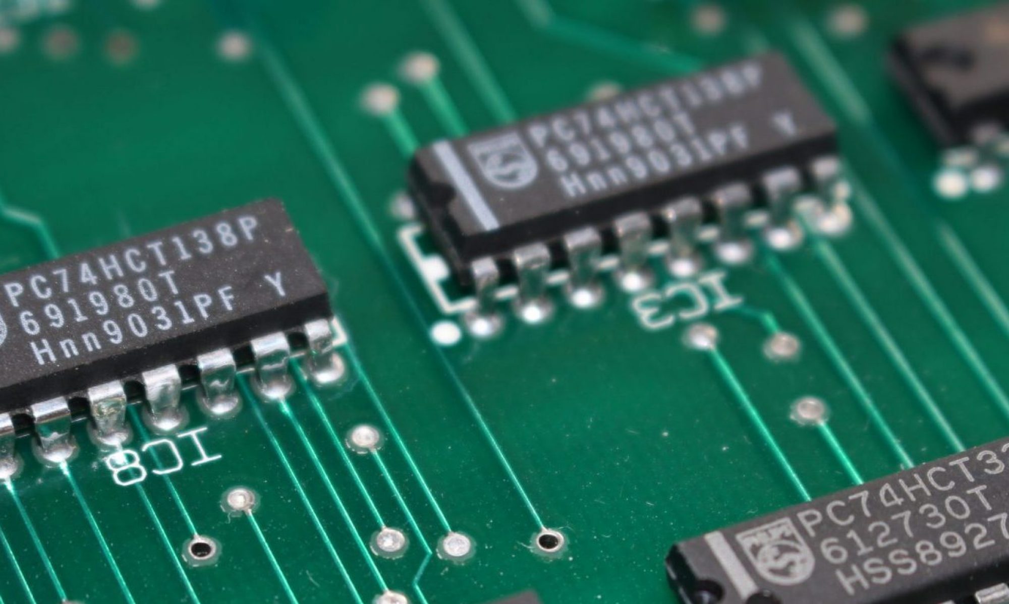
I2C decode of configuration information send to LT3582
Lockdown projects
As the UK moves into another lockdown, I think back to our first one, unbelievably six months ago. Like many engineers, I grasped the opportunity to work on a few personal projects at home, and to further develop skills and knowledge. As a technical writer, I like to keep my skills current and my expertise as practically based as possible. During early April, I bought an STM32 Nucleo L476G development board as the base platform for my projects. I’ve been busy with I2C tutorials, interrupt service routines, using the LSM303AGR MEMS sensor, and the ST MEMS multi-sensor board. I’ve learnt a lot and had some fun. There was no particular reason why I picked the STM32 product family; it just seemed to be complete, with a full IDE, BSPs, and libraries. Everything I wanted was also available from stock.
Opamps next on the list
As the months went by, I was crossing off lots of practical topics from my to-do list. A few weeks ago, I advanced to the next item on the list; opamps. I’d covered them in the distant past when I did my EE exams, but I figured that I ought to revisit them. Given that the humble 741 is in production 57 years since its launch, opamps must still have a purpose.
I started reviewing datasheets and opted to buy some LM358, a device that has become a standardised part made by several manufacturers to the same specification initially developed by National Semiconductor. I’m not sure how old the LM358 is, but it must be similar to the 741 in vintage.
Powering an opamp
Ah, I thought, I’ll probably need a dual rail power supply to power the device, so I’d better find a DC/DC converter to use. I don’t need a negative rail for all projects, but it’s more fun stretching the brief! It didn’t take long to find a compact dual-rail single inductor device, the Linear Technology (now Analog Devices) LT3582. The LT3582 was launched in 2009 and is still in production. Two converters form the architecture of the LT3582, the boost for the positive output, and an inverting one for the negative rail. Device configuration uses a set of I2C registers, and even better, I found a low-cost evaluation board from MikroE.
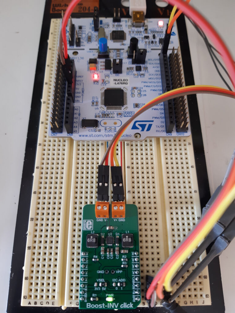
Evaluation board eases prototyping
The MikroE Boost-INV uses the MikroE click board format, a convenient pin layout that caters for power and interfacing. A click board to Arduino Uno shield is available that permits connecting two click boards to an Arduino shield pinout, but I opted to use a breadboard instead.
It didn’t take long to write some code to control the LT3582 from the Nucleo-L476RG, the only minor challenge was that the Boost-INV documentation appears to give the wrong I2C addresses, but an I2C scanner program rectified this reasonably quickly.
The MikroE Boost-INV click board containing an LT3582 and the STM32 Nucleo L476RG
The positive output can be programmed between +3.2 VDC (0x00) to +12.75 VDC (0xBF) in 25 mV steps, and the negative rail from -1.2 VDC (0x00) to -13.95 VDC (0xFF) in 50 mV steps.
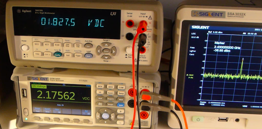
I opted for + 10 VDC and – 10 VDC outputs for which the voltage output control registers REG0 and REG1 were set to 0xB0 and 0x88 respectively. The screen dump from my MSO highlights the process of turning the outputs off, setting the voltages, and re-enabling the output. A soft-start circuitry permits setting a ramp-up of the outputs in a controlled manner to limit peak currents.
In addition to configuring the voltage via I2C, you can also program the LT3582’s settings to be permanent by programming the on-chip non-volatile OTP memory.
Product life cycle planning
Setting up the LT3582 for my opamp projects was really interesting, but it left me wondering how the semiconductor industry deals with product life cycle planning and obsolescence.
The LT3582 is 11 years old; the 741 is 57 years old. At what point does a semi vendor decide to move a component from production to not recommended for new designs. Last time buy, and obsolescence will then follow a prescribed time afterwards. If the device is still selling in significant quantities and the fabrication process is still current, then it must be a hard decision to make. Some devices will be superseded as new iterations become available. There are many factors to consider, including whether a competitor has a similar device still in production.
No doubt statistical analysis of a device’s life cycle yields the basic concepts of product planning as well as determining the likely time frame for obsolescence. There are major differences in some product groups, memory, for example, means it is unlikely a one-size-fits-all approach will work.
What is your viewpoint? How does a product’s availability influence a new design? Please discuss on LinkedIn, and I’ll capture the salient points in my next blog.
In an earlier blog, I highlighted my interest in experimenting with opamps. The speed with which my electronics courses progressed meant we had little time to delve into opamps in depth. I’ve wanted to get back to analogue design basics for some time, having spent a lot of my practical experience and writing time on embedded topics. Having picked up my old amateur radio hobby again has presented the ideal opportunity!
Getting back into using morse code (CW)
It’s been too many years (decades actually) since I used morse code, and I’ve been spending time listening and sending morse on the amateur radio bands. The radio spectrum dedicated to morse code use within the amateur bands tends to become pretty congested during good propagation periods. You need a pretty good audio filter to separate individual signals, typically with a bandpass of 200 Hz centred on 750 Hz. One secondhand receiver I use only has a 1.4 kHz bandpass filter, and unfortunately, despite it being an excellent receiver otherwise, I find it unsuitable for receiving CW signals. Could I build one?
Active filter design options
If you Google how to design an active audio bandpass filter, it will present you with loads of informative pages and tutorials, perhaps even information overload. The majority of ideas promoted the use of opamps. Some results recommended an FPGA and DSP approach, the latter seeming a tad overkill for my skills and available time, not to mention the power consumption profile.
Simulation – see what goes on before you prototype
After researching and reviewing design ideas, I settled on a 4-stage circuit based around the classic 741 opamps favoured by several ham radio bloggers. The centre frequency would be 750 Hz with a 200 Hz (-3dB) passband. But would it work in the way as intended? I didn’t want to resort to building something that didn’t give the flexibility of passband adjustment that I had in my mind. With the passband determined by the RC components in each stage, I wondered if I could use I2C-controlled passives to vary both the passband and the centre frequency. Time to turn to simulation.
I’m an advocate of the merits of simulation to build out knowledge on how a circuit works. You can use simulation techniques for fault-finding, too, if you are not sure how a circuit works in practice.
You’ll find plenty of free simulation tools online. I have both TINA from TI and LTSpice, from Analog Devices on my desktop.
A wizard approach to filter design
Another design approach I considered was the use of an online filter design wizard. Analog Design’s tool is superb.
Figure 1 – Using TI TINA to simulate the design
I like the fact that the Analog Design Filter Wizard provides an overview of the filter method used (Butterworth, Chebyshev etc.), and that you can optimize for low power, low noise, and voltage range. For the rest of this blog, I’m taking the TINA simulation to the next stage, but I’m going to use the wizard approach for implementing a variable passband filter.
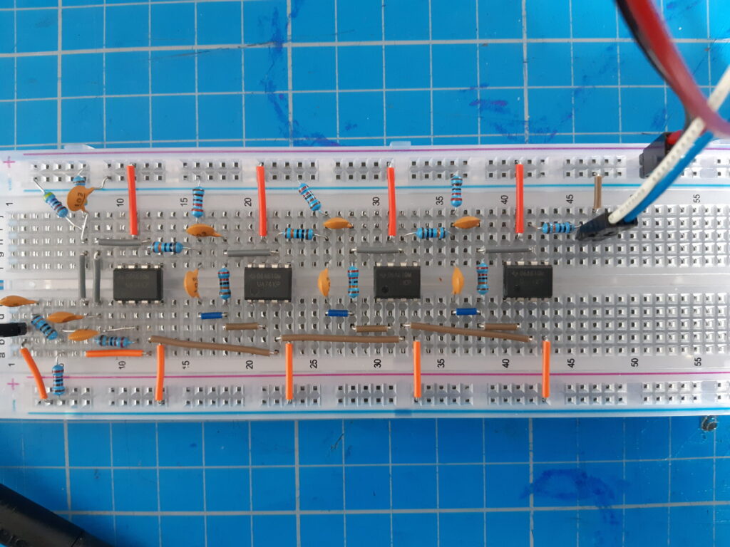
Breadboarding the CW filter
Figure 2 – 4-stage active filter breadboard
Happy with the results of the simulation, I breadboarded the design – see Figure 2. I used TI LM741 opamps, opting for single 8-pin packages to simplify the breadboard layout. https://www.ti.com/product/LM741
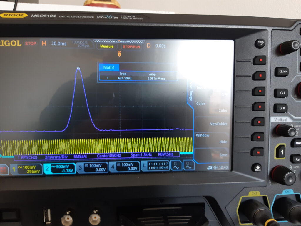
After double-checking the circuit layout, I hooked up a function generator to sweep an unmodulated sine wave from 200 Hz to 1,500 Hz. The supply voltage is 12 VDC with a virtual ground arrangement, and – as seen in Figure 3 – the supply current was only 1.92 mA.
Figure 3 – Function generator settings and power consumption measurement
The output signal was coupled to an oscilloscope, and an FFT function used to trace the filter output. The peak centre frequency identified – see Figure 4 – is 625 Hz, 125 Hz lower than that simulated.
Figure 4 – Filter output showing peak at 625 Hz
Debugging the design
A 625 Hz centre frequency is not unacceptable for practical use. What is causing the difference? My first thoughts involve the tolerance of the components used and the potential for a resistor misplacement. Resistors are all 10%. All the capacitors are the same, so it is unlikely that I’ve used the wrong one.
Part 2
In part 2 of this blog post, I’m going to re-check the components used and their tolerances and, if necessary, update the design. For a variable passband filter, I’m going to base a design around the Analog Design Filter Wizard and investigate the possibility of using I2C controlled passive components.