Designing an active bandpass filter
In an earlier blog, I highlighted my interest in experimenting with opamps. The speed with which my electronics courses progressed meant we had little time to delve into opamps in depth. I’ve wanted to get back to analogue design basics for some time, having spent a lot of my practical experience and writing time on embedded topics. Having picked up my old amateur radio hobby again has presented the ideal opportunity!
Getting back into using morse code (CW)
It’s been too many years (decades actually) since I used morse code, and I’ve been spending time listening and sending morse on the amateur radio bands. The radio spectrum dedicated to morse code use within the amateur bands tends to become pretty congested during good propagation periods. You need a pretty good audio filter to separate individual signals, typically with a bandpass of 200 Hz centred on 750 Hz. One secondhand receiver I use only has a 1.4 kHz bandpass filter, and unfortunately, despite it being an excellent receiver otherwise, I find it unsuitable for receiving CW signals. Could I build one?
Active filter design options
If you Google how to design an active audio bandpass filter, it will present you with loads of informative pages and tutorials, perhaps even information overload. The majority of ideas promoted the use of opamps. Some results recommended an FPGA and DSP approach, the latter seeming a tad overkill for my skills and available time, not to mention the power consumption profile.
Simulation – see what goes on before you prototype
After researching and reviewing design ideas, I settled on a 4-stage circuit based around the classic 741 opamps favoured by several ham radio bloggers. The centre frequency would be 750 Hz with a 200 Hz (-3dB) passband. But would it work in the way as intended? I didn’t want to resort to building something that didn’t give the flexibility of passband adjustment that I had in my mind. With the passband determined by the RC components in each stage, I wondered if I could use I2C-controlled passives to vary both the passband and the centre frequency. Time to turn to simulation.
I’m an advocate of the merits of simulation to build out knowledge on how a circuit works. You can use simulation techniques for fault-finding, too, if you are not sure how a circuit works in practice.
You’ll find plenty of free simulation tools online. I have both TINA from TI and LTSpice, from Analog Devices on my desktop.
A wizard approach to filter design
Another design approach I considered was the use of an online filter design wizard. Analog Design’s tool is superb.

I like the fact that the Analog Design Filter Wizard provides an overview of the filter method used (Butterworth, Chebyshev etc.), and that you can optimize for low power, low noise, and voltage range. For the rest of this blog, I’m taking the TINA simulation to the next stage, but I’m going to use the wizard approach for implementing a variable passband filter.
Breadboarding the CW filter

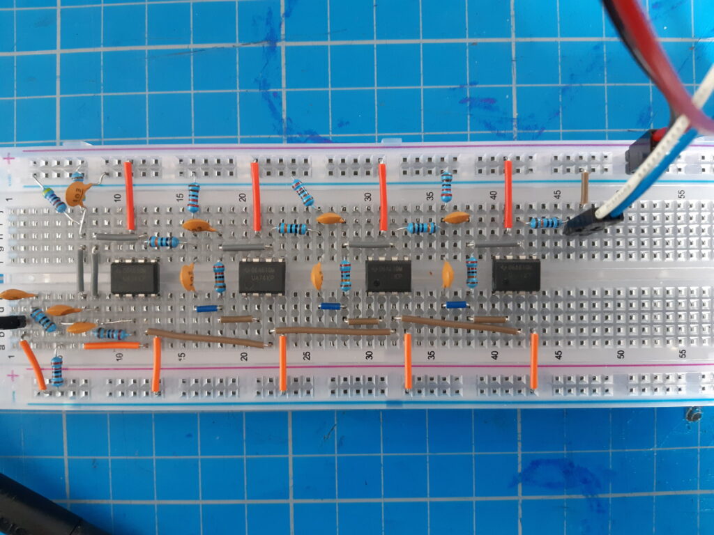
Happy with the results of the simulation, I breadboarded the design – see Figure 2. I used TI LM741 opamps, opting for single 8-pin packages to simplify the breadboard layout.
https://www.ti.com/product/LM741
After double-checking the circuit layout, I hooked up a function generator to sweep an unmodulated sine wave from 200 Hz to 1,500 Hz. The supply voltage is 12 VDC with a virtual ground arrangement, and – as seen in Figure 3 – the supply current was only 1.92 mA.

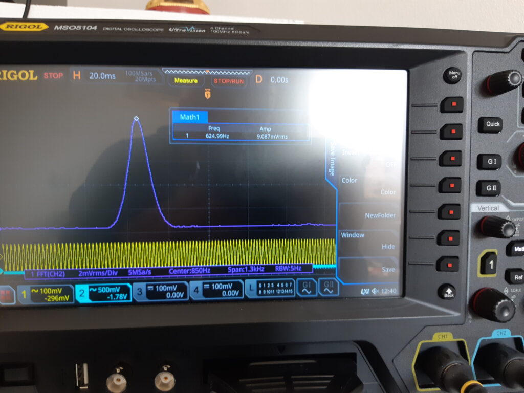
The output signal was coupled to an oscilloscope, and an FFT function used to trace the filter output. The peak centre frequency identified – see Figure 4 – is 625 Hz, 125 Hz lower than that simulated.

Debugging the design
A 625 Hz centre frequency is not unacceptable for practical use. What is causing the difference? My first thoughts involve the tolerance of the components used and the potential for a resistor misplacement. Resistors are all 10%. All the capacitors are the same, so it is unlikely that I’ve used the wrong one.
Part 2
In part 2 of this blog post, I’m going to re-check the components used and their tolerances and, if necessary, update the design. For a variable passband filter, I’m going to base a design around the Analog Design Filter Wizard and investigate the possibility of using I2C controlled passive components.

